- 您现在的位置:买卖IC网 > Sheet目录332 > IR22141SSPBF (International Rectifier)IC DRIVER HALF BRIDGE SGL 24SSOP
IR21141/IR22141SSPbF
Vcc/Vb
R DRp
I avg
C RES
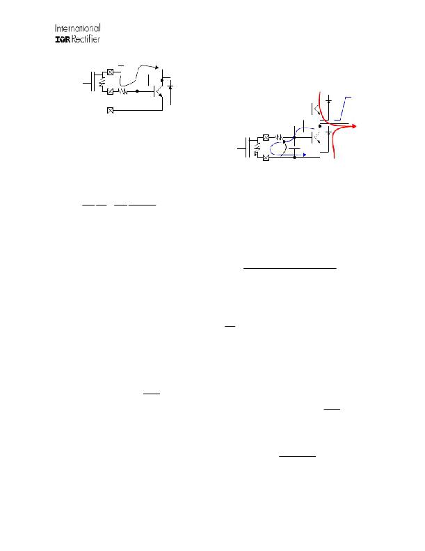
flowing in R Goff and R DRn (see Fig. 22). If the voltage
drop at the gate exceeds the threshold voltage of the
IGBT, the device may self turn on, causing large
oscillation and relevant cross conduction.
R Gon
COM/Vs
Figure 21: R Gon Sizing
HS Turning ON
C RESoff
R Goff
OFF
dV/dt
where
R TOT = R DRp + R Gon
ON
R DRn
C IES
R Gon = gate on-resistor
R DRp = driver equivalent on-resistance
Figure 22: R Goff Sizing: Current Path When Low Side is
R DRp is approximately given by
Off and High Side Turns On
R DRp
? Vcc t SW
? I t
= ? o 1 + on 1
?
? ?
+
Vcc t SW ? t on 1
I o 2 + t SW
Vcc
I o 1 +
for t SW > t on 1
for t SW ≤ t on 1
The transfer function between the IGBT collector and
the IGBT gate then becomes:
V ge s ? ( R Goff + R DRn ) ? C RESoff
=
V de 1 + s ? ( R Goff + R DRn ) ? ( C RESoff + C IES )
(I O1+
,I O2+
and
t on1
from
“Static
Electrical
Characteristics”).
which yields to a high pass filter with a pole at:
Table 1 reports the gate resistance size for two
commonly used IGBTs (calculation made using typical
datasheet values and assuming V CC = 15 V).
1 / τ =
( R Goff
1
+ R DRn ) ? ( C RESoff + C IES )
Output Voltage Slope: The turn-on gate resistor
R Gon can be sized to control the output slope
(dV OUT /dt). While the output voltage has a non-
linear behaviour, the maximum output slope can be
As a result, when τ is faster than the collector rise time
(to be verified after calculation) the transfer function can
be approximated by:
approximated by:
dV out
dt
=
I avg
C RESoff
V ge
= s ? ( R Goff + R DRn ) ? C RESoff
V de
so that
Vcc ? V ge
C RESoff ?
V ge = ( R Goff + R DRn ) ? C RESoff ?
V th > V ge = ( R Goff + R DRn ) ? C RESoff
inserting the expression yielding I avg and rearranging:
*
R TOT =
dV out
dt
As an example, table 2 shows the sizing of gate
resistance to get dV out /dt= 5 V/ns when using two
popular IGBTs (typical datasheet values are used and
V CC = 15 V is assumed).
dV de
dt
in the time domain. Then the condition:
dV out
dt
must be verified to avoid spurious turn on.
Rearranging the equation yields:
NOTICE : Turn on time must be lower than T BL to avoid
improper desaturation detection and SSD triggering.
2.6 Sizing the Turn-Off Gate Resistor
The worst case in sizing the turn-off resistor R Goff is
R Goff <
V th
C RESoff
?
dV
dt
? R DRn
when the collector of the IGBT in the off state is forced
to commutate by an external event (e.g., the turn-on of
the companion IGBT). In this case the dV/dt of the
output node induces a parasitic current through C RESoff
www.irf.com
19
R DRn is approximately given by
? 2009 International Rectifier
发布紧急采购,3分钟左右您将得到回复。
相关PDF资料
IR2235JPBF
IC DRIVER BRIDGE 3PHASE 44PLCC
IR2301PBF
IC DRIVER HIGH/LOW SIDE 8DIP
IR2302PBF
IC DRIVER HALF BRIDGE 8DIP
IR2304SPBF
IC DRIVER HALF BRIDGE 8-SOIC
IR2308SPBF
IC DRIVER HALF BRIDGE HV 8SOIC
IR3101
IC POWER MODULE 1.6A 500V 11-SIP
IR3103
PWR MOD 180W GATE DRIVER 11-SIP
IR3519STRPBF
IC MOSFET GATE DRIVER SON-8
相关代理商/技术参数
IR22141SSPBF
制造商:International Rectifier 功能描述:Driver IC
IR22141SSTRPBF
功能描述:功率驱动器IC Hlf Brdg Drvr IC for Pwr Swtch App RoHS:否 制造商:Micrel 产品:MOSFET Gate Drivers 类型:Low Cost High or Low Side MOSFET Driver 上升时间: 下降时间: 电源电压-最大:30 V 电源电压-最小:2.75 V 电源电流: 最大功率耗散: 最大工作温度:+ 85 C 安装风格:SMD/SMT 封装 / 箱体:SOIC-8 封装:Tube
IR2214SS
功能描述:IC DRIVER HALF BRIDGE SGL 24SSOP RoHS:否 类别:集成电路 (IC) >> PMIC - MOSFET,电桥驱动器 - 外部开关 系列:- 标准包装:50 系列:- 配置:高端 输入类型:非反相 延迟时间:200ns 电流 - 峰:250mA 配置数:1 输出数:1 高端电压 - 最大(自引导启动):600V 电源电压:12 V ~ 20 V 工作温度:-40°C ~ 125°C 安装类型:通孔 封装/外壳:8-DIP(0.300",7.62mm) 供应商设备封装:8-DIP 包装:管件 其它名称:*IR2127
IR2214SSPBF
功能描述:功率驱动器IC 1200V HALF BRDG DRVR IC RoHS:否 制造商:Micrel 产品:MOSFET Gate Drivers 类型:Low Cost High or Low Side MOSFET Driver 上升时间: 下降时间: 电源电压-最大:30 V 电源电压-最小:2.75 V 电源电流: 最大功率耗散: 最大工作温度:+ 85 C 安装风格:SMD/SMT 封装 / 箱体:SOIC-8 封装:Tube
IR2214SSPBF
制造商:International Rectifier 功能描述:Driver IC
IR2214SSTRPBF
功能描述:功率驱动器IC Hlf Brdg Drvr IC for Pwr Swtch App RoHS:否 制造商:Micrel 产品:MOSFET Gate Drivers 类型:Low Cost High or Low Side MOSFET Driver 上升时间: 下降时间: 电源电压-最大:30 V 电源电压-最小:2.75 V 电源电流: 最大功率耗散: 最大工作温度:+ 85 C 安装风格:SMD/SMT 封装 / 箱体:SOIC-8 封装:Tube
IR2233
功能描述:IC DRIVER 3-PHASE BRIDGE 28-DIP RoHS:否 类别:集成电路 (IC) >> PMIC - MOSFET,电桥驱动器 - 外部开关 系列:- 标准包装:50 系列:- 配置:低端 输入类型:非反相 延迟时间:40ns 电流 - 峰:9A 配置数:1 输出数:1 高端电压 - 最大(自引导启动):- 电源电压:4.5 V ~ 35 V 工作温度:-40°C ~ 125°C 安装类型:表面贴装 封装/外壳:TO-263-6,D²Pak(5 引线+接片),TO-263BA 供应商设备封装:TO-263 包装:管件
IR2233J
功能描述:IC DRIVER 3-PHASE BRIDGE 44-PLCC RoHS:否 类别:集成电路 (IC) >> PMIC - MOSFET,电桥驱动器 - 外部开关 系列:- 标准包装:50 系列:- 配置:低端 输入类型:非反相 延迟时间:40ns 电流 - 峰:9A 配置数:1 输出数:1 高端电压 - 最大(自引导启动):- 电源电压:4.5 V ~ 35 V 工作温度:-40°C ~ 125°C 安装类型:表面贴装 封装/外壳:TO-263-6,D²Pak(5 引线+接片),TO-263BA 供应商设备封装:TO-263 包装:管件
